Description
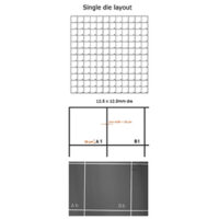
The novel EM-Tec FG1 silicon SEM finder grid substrate consists of an a 12x12mm chrome deposited grid with a 1mm pitch on a conductive ultra-flat silicon substrate. The substrate is divided into 144 indexed fields of 1x1mm where each of the fields has a unique alphanumeric label in the lower right corner. The alphanumeric label is easy to see with a magnifier, stereo microscope and/or SEM. The grid produced is comparable with 25 mesh and is practical for larger particles or small samples mounted on the substrate in separate fields. The EM-Tec FG1 silicon SEM finder grid substrate is ideal for correlative microscopy since the position of the sample is easily located. Size of the EM-Tec FG1 is 12x12mm on a 12.5 x 12.5mm substrate. Primarily designed for SEM applications, but equally suitable for reflected light microscopy, AFM and Auger/SIMS._x000D_
_x000D_
This unique product has a number of advantages over engraved SEM stubs and the usual copper SEM finder grids:_x000D_
– Ultra-flat – no height differences such as with copper finder grids_x000D_
– Pattern is easily visible with unaided eye, SEM and light microscope_x000D_
– Each individual field indexed with an alphanumeric label_x000D_
– Low background signal for SEM imaging – similar to Si chips_x000D_
– Fine bright pattern over entire area – finer than engraved stubs_x000D_
– Sample size can be easily judged with the 1x1mm pattern in the background_x000D_
– Compatible with Ø12.7mm pin stubs, Ø12.2mm JEOL stubs and Ø15mm Hitachi stubs_x000D_
– Easy to mount on SEM and AFM stubs_x000D_
– Compatible with SEM, FIB, AFM, LM, XPS/ESCA, SIMS and Auger_x000D_
– Reusable – solvent resistant and plasma cleaning compatible_x000D_
– The EM-Tec FG1 silicon SEM finder grid substrate in packaged in a clean-room and shipped in a gel-box._x000D_
_x000D_
The EM-Tec FG1 finder grid is ideal for:_x000D_
– correlative, corroborative, collaborative and repetitive microscopy_x000D_
– multi-sample mounting for small samples_x000D_
– demonstration samples with quick finder grid_x000D_
– quick size estimation with the 1mm grid_x000D_
_x000D_
Specifications of the pattern and the ultra-flat silicon wafer of the EM-Tec FG1 silicon finder grid:_x000D_
_x000D_
_x000D_
_x000D_
| Pattern size | _x000D_
12 x12 mm divided into 144 individual 1x1mm fields | _x000D_
_x000D_
_x000D_
| Numbering | _x000D_
Each field has unique alphanumeric label in lowe right corner | _x000D_
_x000D_
_x000D_
| Pattern/labels | _x000D_
75nm thick deposited Cr with 20µm line width, 80µm label height | _x000D_
_x000D_
_x000D_
| Substrate size | _x000D_
12.5×12.5mm | _x000D_
_x000D_
_x000D_
| Orientation | _x000D_
<100> | _x000D_
_x000D_
_x000D_
| Type | _x000D_
P (Boron) | _x000D_
_x000D_
_x000D_
| Resistance | _x000D_
1-10 Ohm/cm | _x000D_
_x000D_
_x000D_
| Grade | _x000D_
Prime / CZ Virgin | _x000D_
_x000D_
_x000D_
| Coating | _x000D_
None, native oxide only | _x000D_
_x000D_
_x000D_
| Thickness | _x000D_
675µm (+/- 20µm) | _x000D_
_x000D_
_x000D_
| TTV | _x000D_
≤1.5µm | _x000D_
_x000D_
_x000D_
| Warp | _x000D_
≤30µm | _x000D_
_x000D_
_x000D_